> Energy band gap>
GaAs |
AlxGa1-xAs |
InxGa1-xAs
> Refractive index
> GaAs |
AlAs |
AlxGa1-xAs |
InxGa1-xAs
> Devices
> Bragg mirror |
SAM |
RSAM |
SA |
SANOS |
SOC |
Microchip |
PCA
> Device application
> Papers |
Patents |
FAQs
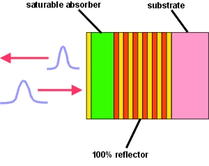
SAM - Saturable Absorber Mirror
SAM construction and application
Construction:
- The SAM consists of a mirror and a saturable absorber in front of it.
- The single crystalline layers of the mirror and the absorber are grown on a GaAs wafer.
Behaviour:
- The SAM is a nonlinear mirror.
- The reflectance increases with increasing pulse energy.
Application:
- Using a saturable absorber mirror (SAM), a self-starting, passively mode-locked diode pumped laser with a very stable pulse repetition rate can be realized.
- SAMs for solid state and fiber lasers in a wide spectral region from 800 nm up to 3 µm wavelength are available.
- Also Q-switched mircochip lasers can be realized using a SAM as nonlinear optical device.
• Time dependent absorption
Time dependent absorption
We consider the saturable absorber as a two level system. The electrons in the valence band of the semiconductor absorber material are in their ground state and can be excited into the conduction band when photons with energy E = h·ν are absorbed.
If the number of states in the valence band is NV and in the conduction band NC then during the illumination of the absorber the rate of transitions between the two states can be described as
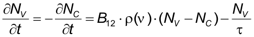
- NV - number of states in the valence band
- NC - number of states in the conduction band
- B12 = B21 – Einstein B coefficient
- ρ(ν) - density of incident photons
- τ - relaxation time of the excited electrons in the conduction band.
The excited electrons in the conduction band relax either by spontaneous photon emission or by non-radiative energy loss with a mean
relaxation time constant τ.
The sum of states in the valence and conduction band gives the total number of electrons NT which take place on the absorption process: NT = NV + NC.
Without illumination of the absorber all electrons are in the ground state NC = NT. In case of very high density of incident photons the
maximum value for the excited states NC=NV=NT/2 is approached and the absorber is transparent.
The absorption A of the saturable absorber is proportional to the number of electrons NC in the ground state. If we consider that the incident photon density is proportional
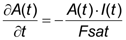
to the time dependent optical beam intensity I(t) then we can rewrite the rate equation for the number of states into a rate equation for the absorption A(t) as
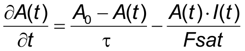
- A0 – non-saturated absorption, if NC = NT/li>
- I(t) - time dependent optical beam intensity/li>
- Fsat = I(t)/(B12ρ(ν)) - saturation fluence of the absorber.
The arbitrary solution of this differential equation for saturable absorption A(t) is
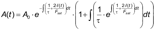
- A(t) – time dependent absorption.
For a certain time dependency of the optical pulse intensity I(t) the integration in the exponential function can be carried out.
In case of a Gaussian pulse the intensity I(t) can be written as
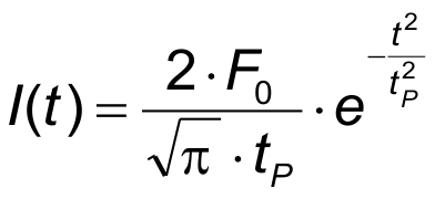
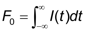
- F0 – pulse fluence
- tP - pulse duration.
The integration in the exponential function can be executed resulting in the following time dependent absorption A(t)
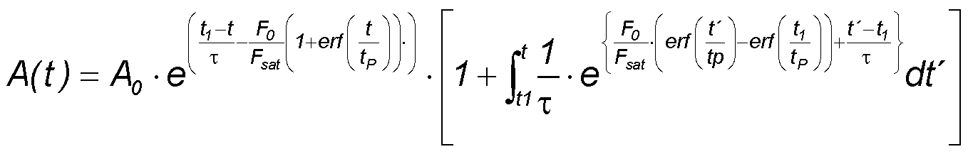
for t1<< - tP
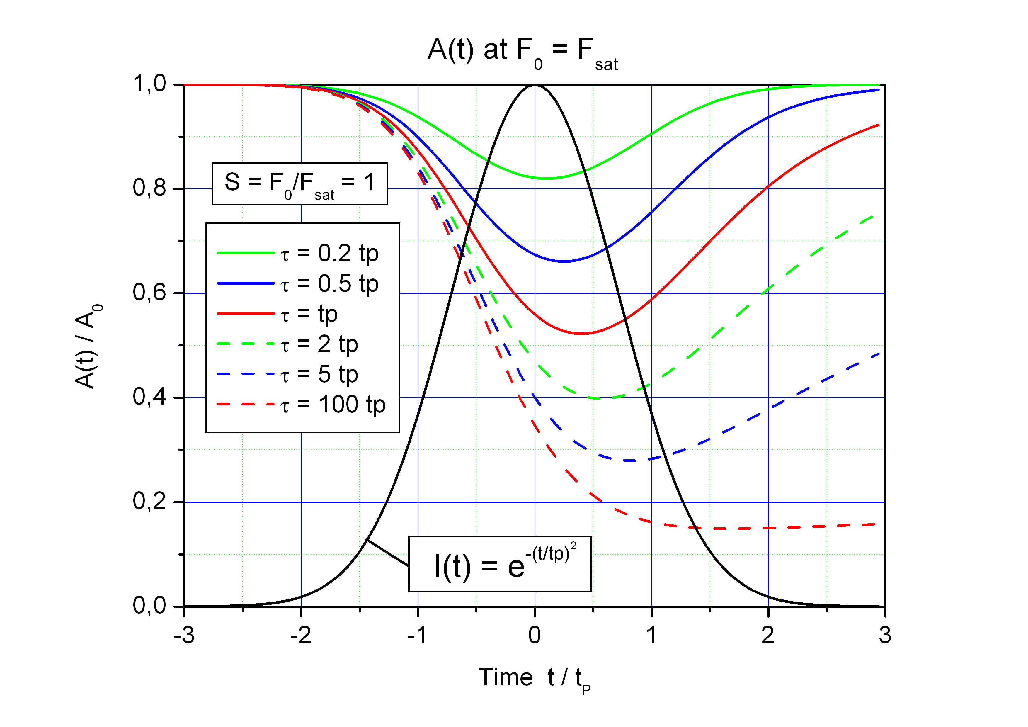
Time dependent saturation of the absorption A(t)/A0 for F0 = Fsat and different
absorber relaxation time τ. Black curve: Gaussian pulse I(t).
tP - pulse duration.
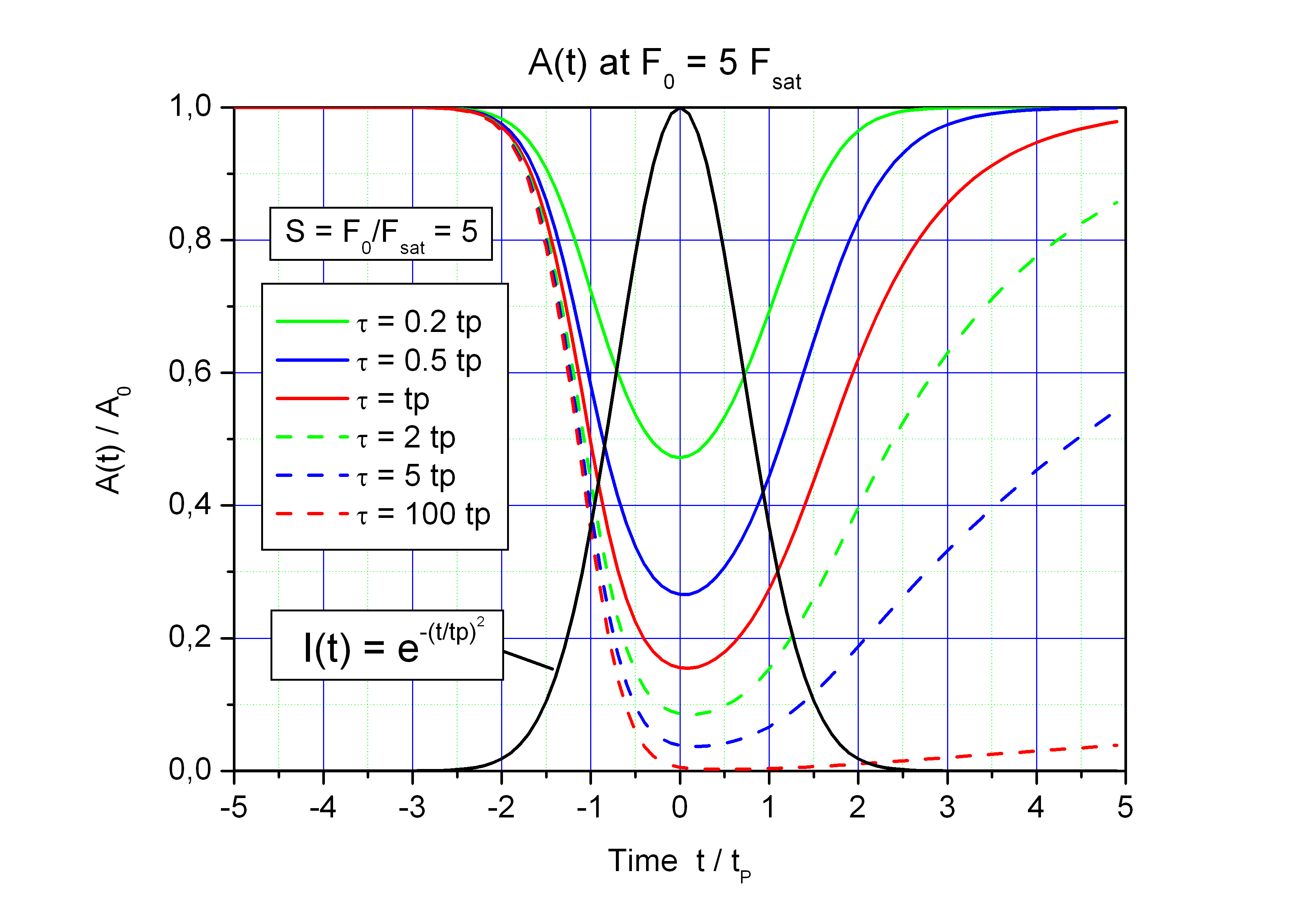
Time dependent saturation of the absorption A(t)/A0 for F0 = 5·Fsat and different
absorber relaxation time τ. Black curve: Gaussian pulse I(t).
tP - pulse duration.
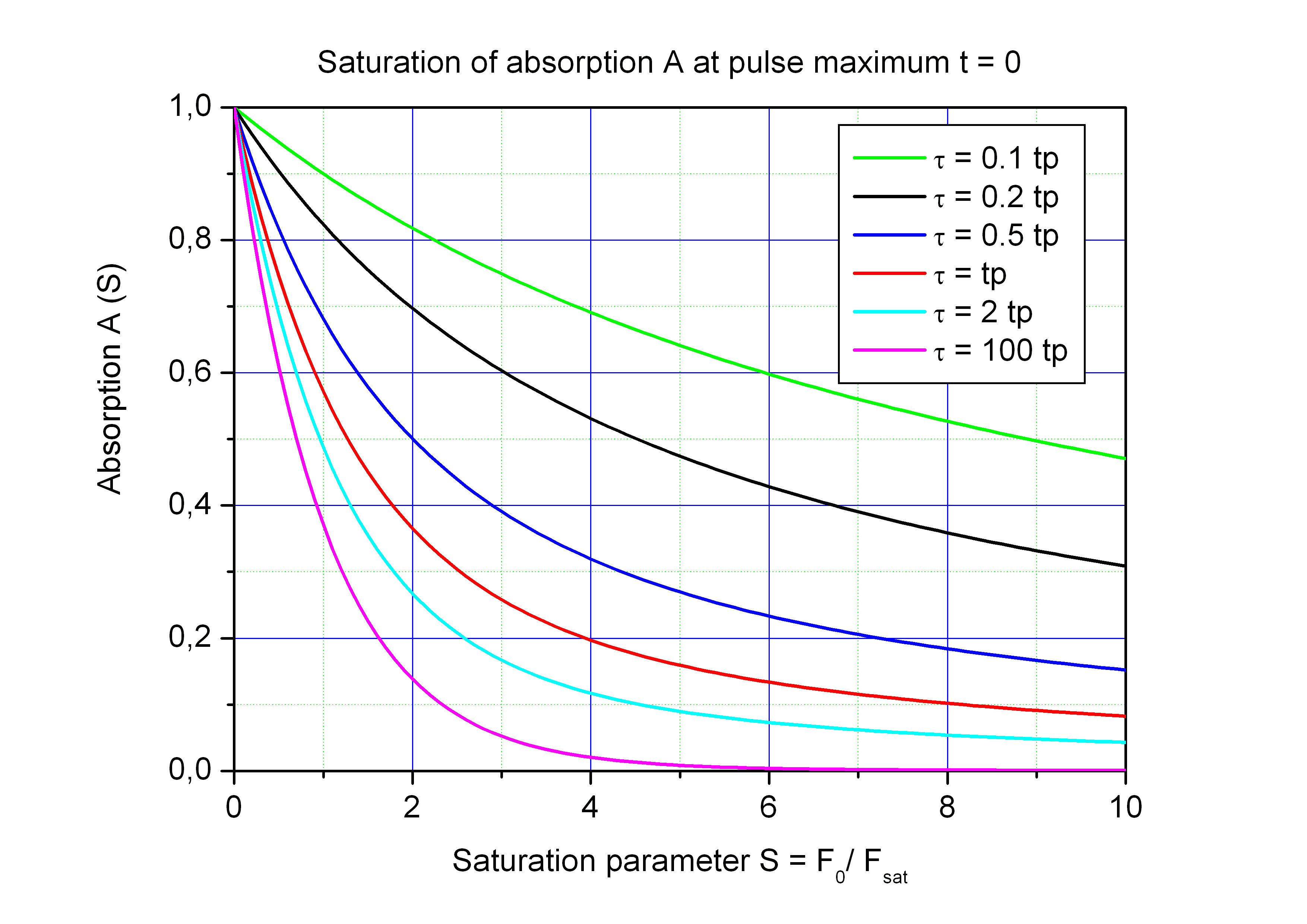
The saturation curve A(F) can be calculated with the above equation A(t) for a certain time, for instance at the pulse maximum.
S = F0/Fsat is the saturation parameter.
Saturation of the absorption A for different ansorber relaxation time τ at the fixed time of pulse maximum t = 0.
In case of a short absorber relaxation time τ << tP the modulation depth of the absorber is significantly reduced.
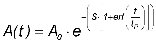
Approximation for long relaxation time τ >> tP
In this case the relaxation term in the rate equation for the absorption can be neglected and the following equation can be used:
 with the solution
 .
.
For a Gaussian pulse the integration delivers
 .
.
- A(t) - time dependent absorption
- A0 - low intensity absorption
- S = F0 / Fsat - saturation parameter
- tP - pulse duration.
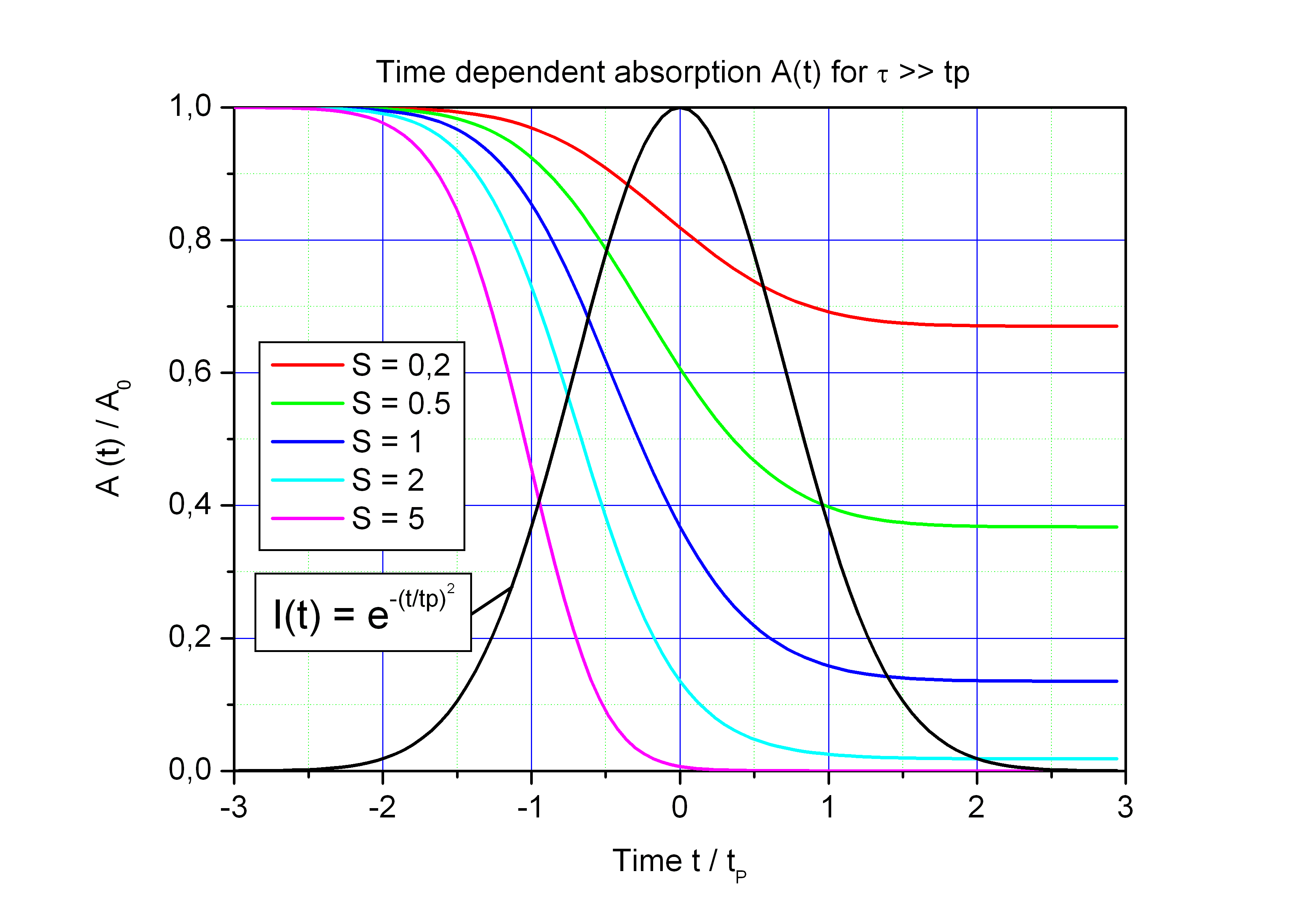
Time dependent absorption A(t)/A0 for different saturation parameters S = F0/Fsat. Black curve: pulse I(t)·tP/F0.
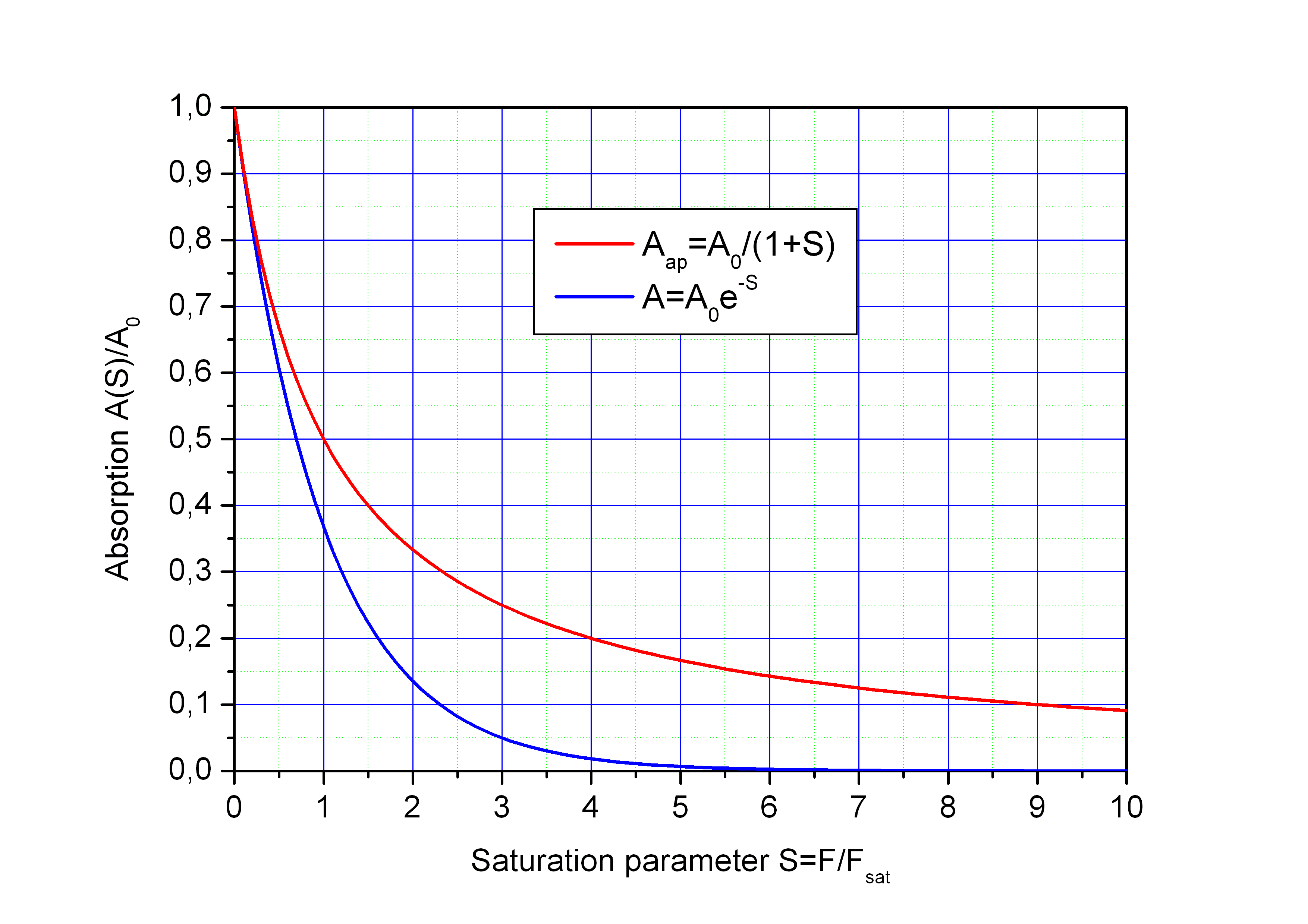
Saturation curve
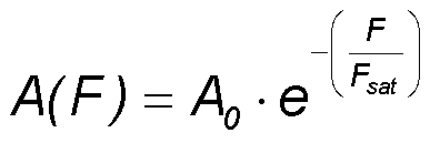
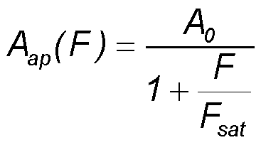
For t >> tP we get the following saturation curve under the above mentioned condition τ >> tP:
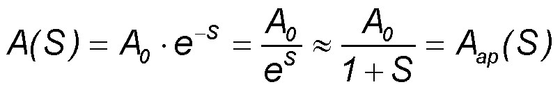
with saturation parameter S = F0/Fsat.
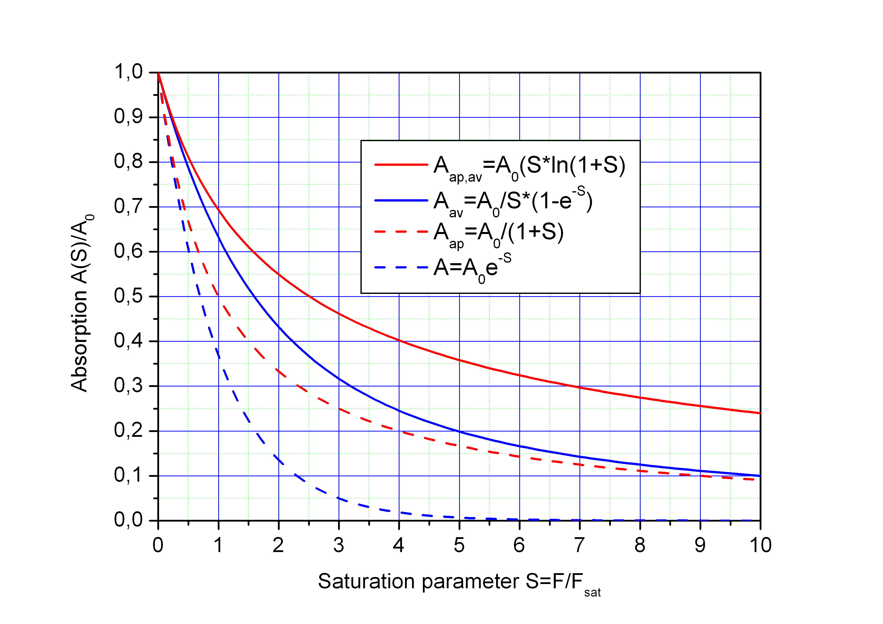
Comparison of the saturation curve A(S)/A0 for the exact solution A = A0·e-S (blue curve) and the approximation A = A0/(1+S) (red curve).
Approximation for short relaxation time τ << tP
In this case the dependency dA/dt in the above rate equation for the absorption A can be neglected because at each time the absorption is determined solely by the actual optical intensity I(t) and not on its history.
for τ << tP
The effective saturation is reduced by the ratio τ/tP. For the use of the saturable absorber as mode-locker this case must be avoided because of the reduced modulation depth.
• Spatial averaged saturation
Spatial averaged saturation
The pulse fluence of a Gaussian beam depends on the distance r from beam axis (r = 0) and can be written as:
- F(r) - radial dependency of the pulse fluence
- r - distance to the beam axis
- F0 - pulse fluence on the beam axis
- r0 - beam radius.
We consider the case of slow absorber relaxation τ >> tP (τ - relaxation time of excited electrons, tP – pulse duration). The spatially averaged absorption over a Gaussian beam can be calculated by
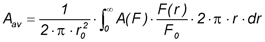
Saturation of absorption
Fsat - saturation fluence of the absorber
Approximated saturation of absorption
Result of the above averaging with the saturation parameter S=F0/Fsat
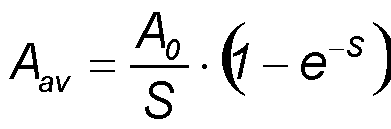
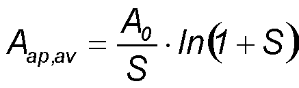
Saturation of absorption A(S) non-averaged (dashed curves) and averaged (full curves) for the exact solution
of the rate equation (blue) and for the approximation (red).
The spatial averaging over a Gaussian beam results in a reduction of the modulation depth like a non-saturable absorption.
• TPA - Two Photon Absorption
TPA - Two Photon Absorption
Two photon absorption must be considered in case of short pulses, especially if the pulse duration tP is < 1 ps.
The two-photon absorption ATPA increases the total absorption as follows:
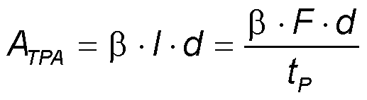
with
- β - two-photon absorption coefficient
- I - pulse intensity
- d - absorber layer thickness
- F - pulse fluence
- tP - pulse duration.
The integration of the time dependent intensity I(t) over the pulse duration tP results in the pulse fluence F.
Therefore the pulse fluence can be approximated as F ~ I · tP.
The two-photon absorption coefficient β is a material dependent parameter. For GaAs the value is β = 2.5·10-10 m/W.
• Ans - non-saturable absorption
Ans - non-saturable absorption
The main reason for a measured non-saturable absorption is two photon absorption (TPA), mainly in case of short pulses.
But also the following two effects result in a similar increase of the measured absorption:
- Temperature increase in the absorber material with increasing pulse fluence during a saturation measurement. This may result in an inceasing measured absorption with inceasing pulse fluence but it is a secondary effect and not a really non-saturable absorption.
- If the pulse duration in a saturation measurement is longer then the shortest relaxation time of the absorber material then a "non-saturable" amount of absorption is obtained. But this is solely the result of a too long measurement pulse and not really a non-saturable absorption.
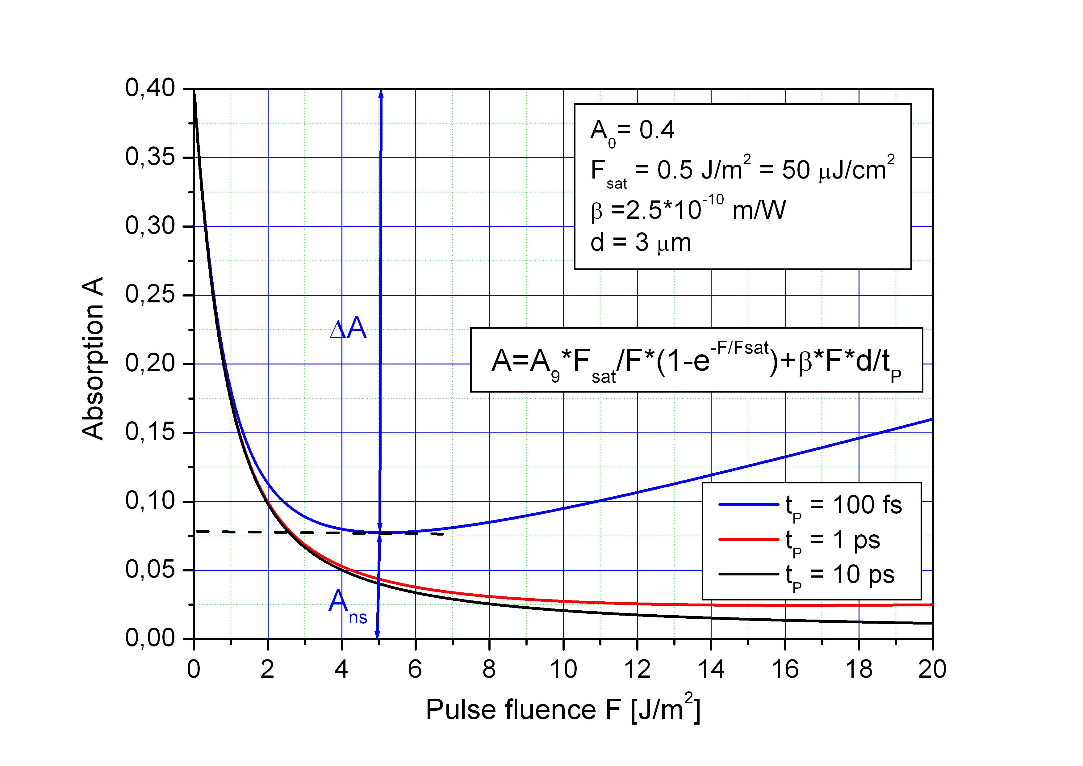
If TPA is relevant in case of short pulses then the absorber relaxation time τ will be also large in comparison to pulse duration tP. This means τ >> tP and the above mentioned formula for the spatial averaged saturable absorption A = A0/S·(1-e-S) can be used. Then the fluence dependent absorption can be written as sum of saturable absortion and TPA:
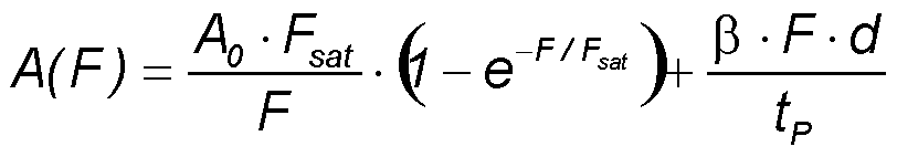
- F - pulse fluence
- A0 - low intensity absorption
- Fsat - saturation fluence
- β - two-photon absorption coefficient
- d - absorber layer thickness
- tP - pulse duration.
The figure shows how the TPA results in a non-saturable absorption Ans in case of short pulses. The non-saturable absorption increases with decreasing pulse duration tP<7sub<.
A0 = ΔA + Ans
TPA can help to stabilize continuous wave mode-locking in short pules lasers because it limits the maximum pulse energy and reduces Q-switch mode-locking to the range of low pump power level.
• SAM reflectance
SAM Reflectance
The saturable absorber mirror (SAM) has no transmission in the stop band of the Bragg mirror. Therefore the reflectance is R = 1 - A.
If two photon absorption (TPA) is included and the absorber relaxtion time τ is short in comparison to the
pulse duration tP then the laterally averaged saturation of the SAM reflectance R can be calculated by
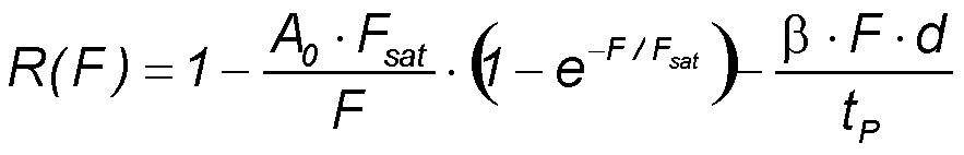
- A0 - low intensity absorption
- F - pulse fluence
- Fsat - saturation fluence
- β - two-photon absorption coefficient
- d - absorber layer thickness
- tP - pulse duration.
The figures below show the reflectance of a SAM with A0 = 0.4, Fsat = 0.5 J/m2 and an absorber thickness d = 3 µm as a function of the pulse fluence F for three different pulse durations tP in a linear and a logarithmic scale.
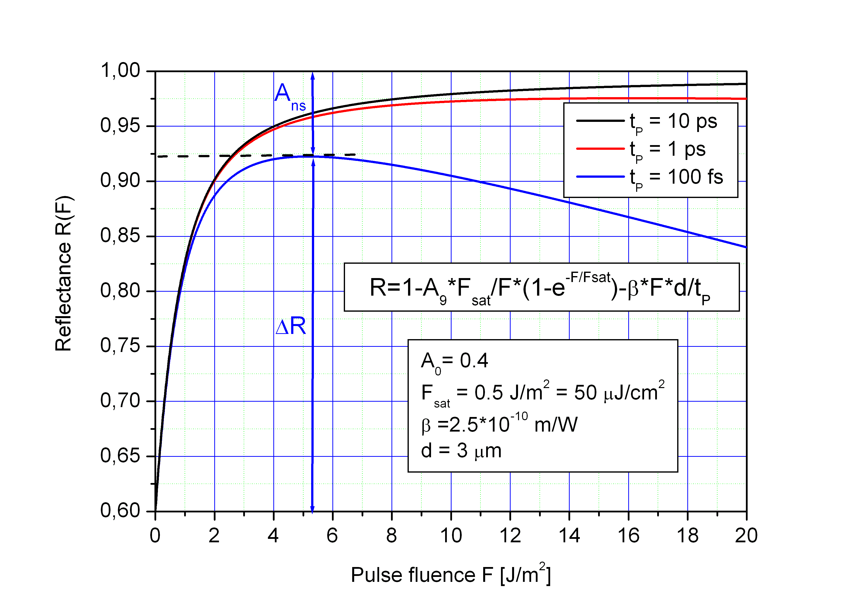
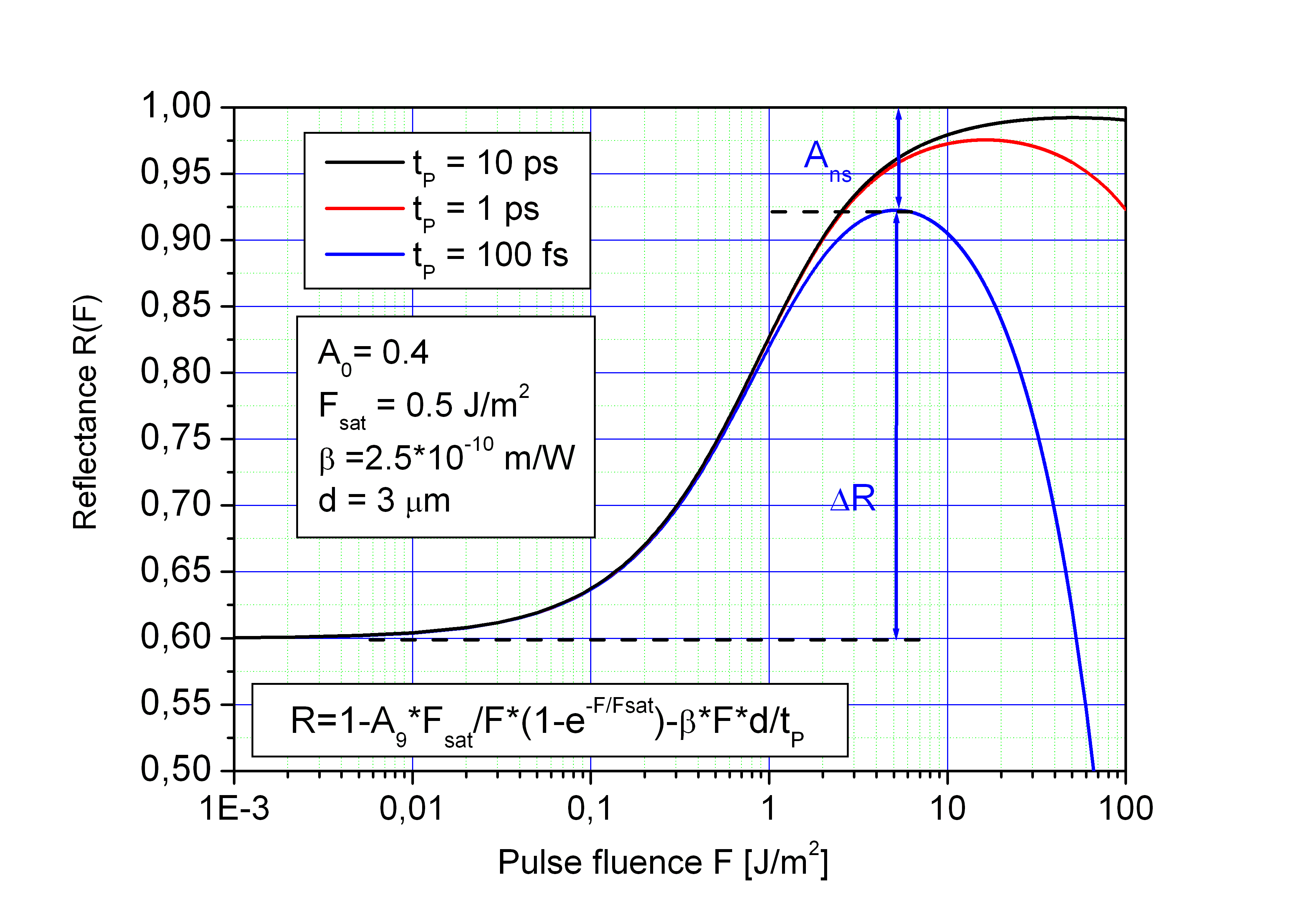
Modulation depth
The modulation depth ΔR is smaller then the low intensity absorption A0 and depends on the
pulse duration because of TPA (two photon absorption) in the absorber and the Bragg mirror.
The TPA coefficient β depends on the material. It increases
with decreasing energy gap of the semiconductor material and can be only estimated because of the
different materials in the absorber layer and Bragg mirror
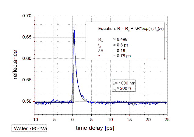
• Relaxation time
Relaxation time τ
The saturable absorber layer consists of a semiconductor material with a direct
band gap slightly smaller than the photon energy of the laser beam. As a result of photon absorption
electron-hole pairs are created in the absorber film.
For laser mode-lockig the relaxation time τ of the excited carriers shall be
somewhat longer than the pulse duration. In this case the back side of the pulse is still free of absorption, but during the
whole period between two consecutive pulses the absorber is non saturated and serves for a high absorption.
Because the relaxation time due to the spontaneous photon emission in a direct
semiconductor is about 1 ns, some precautions has to be done to shorten it for mode-locking application.
Two technologies are used to introduce lattice defects in the absorber layer for fast non-radiative relaxation of excited carriers:
- low-temperature molecular beam epitaxy (LT-MBE)
- ion implantation.
The parameters to adjust the relaxation time in both technologies are the growth temperature in case of LT-MBE and the ion dose in case of implantation. Typical values of the relaxation time τ of SAMs are between 500 fs and 30 ps.
An example of a pump-probe measurement to determine the relaxation time τ is shown right.
• Saturation fluence
Saturation fluence Fsat
The saturation fluence Fsat depends on the semiconductor material and the
optical design of the SAM. Low saturation fluence has the advantage that the laser mode-locking
can be started at low power level. This avoids a fast absorber degradation
For decreasing the saturation fluence the thickness of the semiconductor absorber layer
is reduced below ~ 10 nm. In this case a quantization of the electron energy and the momentum
in the direction perpendicular to the absorber layer takes place and as a consequence the
density of states decreases below the value of a compact semiconductor. Therefore the absorber layers
in a SAM are thin quantum wells with a smaller band gap than the barriers on both sides. If a
larger absorption value of the SAM is needed, the number of the quantum wells is increased instead of
using a single thick absorber layer.
The electric field intensity in front of the Bragg mirror of a SAM is a periodic function with nodes
and antinodes. The absorbing quantum wells are positioned in the antinodes to get a low
saturation fluence. Together with the Fresnel reflectance at the semiconductor-air boundary
the Bragg mirror builds a Fabry-Perot like resonator, which contains the quantum wells.
The optical thickness of the semiconductor material between the reflectors determines the cavity
to be resonant or anti-resonant. The saturation fluence of a resonant SAM is lower than that
of an anti-resonant SAM because of the field enhancement inside the cavity.
Typical saturation fluence of a resonant SAM is Fsat ~ 30 µJ/cm² = 0.3 J/m² whereas
the saturation fluence of an anti-resonant SAM is Fsat ~ 120 µJ/cm² = 1.2 J/m²
• Influence of absorber temperature
Influence of absorber temperature
The SAM parameters depend on the temperature mainly because of two effects:
- Thermal expansion of the absorber material
- Decrease of the semiconductor band gap with increasing temperature.
Temperature dependent optical thickness ot
The second effect results in an increase of komplex refractive index n+i·k with increasing temperature. Together with the
thermal expansion this leads to an increase of optical thickness n·d (n - real part of refractive index, d - film thickness)
with temperature. Therefore with increasing temperature shifts the spectral reflection curve of the SAM towards longer wavelengths.
This thermal shift can be measured for a typical SAM consisting of AlAs, GaAs and InGaAs layers. The temperature coefficient
for the optical thickness can be determined to
αot ~ 7·10-5/K.
This value is substantial larger then the linear thermal expansion coefficient αt = 5.39·10-6/K
of GaAs and therefore mainly determined by the change of the band gap and the refractive index.
A temperature shift of the SAM spectral curve can be calculated using the relation
n·d(T) = n·d(T0 + ΔT) = n·d(T0) · (1 + αot · ΔT)
orΔ(n·d) = n·d(T0) · αot · ΔT
with
- n·d - optical thickness
- T0 - reference temperature
- ΔT = T - T0 - temperature difference
- αot - temperature coefficient for optical thickness
- Δ(n·d) - optical thickness difference.
A temperature rise of 100 K shifts the SAM spectral curve towards longer wavelengths by 7 nm at 1 µm wavelength and by 21 nm at 3 µm. Such a shift is important in case of a resonant SAM.
Temperature dependent absorption
The imaginary part k of the refractive index and consequently the absorption of a direct semiconductor increases with temperature.
This is also a consequence of decreasing band gap with increasing temperature.
For a typical SAM the temperature coefficient of the imaginary part k of the refractive index is
αk ~ 6·10-3/K.
With this coefficent the temperature dependent value for k can be calculated by
k(T) = k(T0)·(1+αk·ΔT)
Therefore k and also the SAM absorption increase by 50 % if the absorber temperature increases by 83 K. This temperature dependence has a significant influence on laser mode-locking.
• Absorber temperature
Absorber temperature
The saturable absorber converts a part of the incoming photon energy into heat. This thermal energy increases the absorber
layer temperature during and shortly after an optical pulse. After that the heat is transported through the substrate to
the heat sink on the rear substrate side. In case of a substrate like GaAs with a high thermal conductivity only a negligible
amount of the dissipated heat goes trough the front surface of the absorber into air.
In case of a pulsed laser beam the absorber temperature T varies periodically with the pulse repetition rate f. A continuous
heat flow from the absorber layer to the heat sink leads to a constant absorber temperature rise ΔTstat.
The heat diffusion into the GaAs substrate and the resulting temperature distribution T(r,t) can be described by the heat diffusion equation (1)
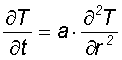
eq. (1) with a - thermal diffusivity (3.1·10-5 m²/s for GaAs)
If the laser spot radius r on the absorber surface is small in comparison to the substrate thickness (typically 0.5 mm)
then the heat flow in the absorber layer is nearly one dimensional but in the substrate three dimensional
(with a point source). Then the heat is distributed into a half space of the substrate resulting in a temperature field
with nearly concentric interfaces of equal temperature.
If we consider at first the time average temperature increase delta Tstat of the absorber layer caused by the mean absorbed
optical power Pm, then we can use the following relations for a centre symmetric three dimensional heat flow (eq. 2)

- λ - thermal conductivity
- ri - inner (illuminated) radius of a sphere
- ro - outer radius of a sphere
- T0 - heat sink temperature
The approximation used is ri « ro when we consider the GaAs wafer thickness as ro substantial larger then the laser spot radius ri=r. Then the mean absorbed optical power is
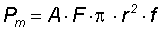
eq.(3) with
- Pm - mean absorbed optical power
- A - absorptance of the absorber
- r - spot radius on the absorber
- f - optical pulse repetition rate.
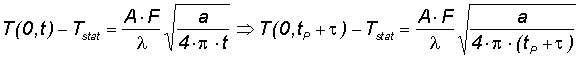
To take into account that the heat flow is only into a half space (not to air) and that in the vicinity of the absorber layer the flow is nearly one dimensional (not three dimensional as calculated) the real temperature rise is about by a factor of 4 higher then in the above equation (2), so that
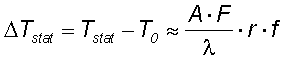
eq. (4) with
- ΔTstat - static temperature rise
- F - pulse fluence
- λ - thermal conductivity,(55 W/(mK) for GaAs)
If the laser spot radius r is larger then the substrate thickness d then the heat flow is nearly one dimensional and then
r must be replaced by d in the above equation (4).
The time dependent solution of the one dimensional heat equation within the absorber layer can be estimated using the response
of the system on a Dirac delta function, which simulates the heating at z=0 during a short laser pulse. The temperature
evaluation near the surface (z² < 4at) after the laser pulse at t>tp can be written in this case as
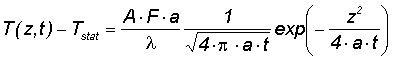
eq. (5) with
- z - coordinate in heat flow direction
- t - time after optical pulse
- a - thermal diffusivity.
Here the heated volume after the laser pulse is approximated by the product of the illuminated area
and the diffusion length (4at)1/2.
The maximum temperature of the absorber layer at z=0 can be expected after the absorbed optical energy is converted into heat.
This is roughly after the sum of the pulse duration tp and the carrier relaxation time τ
eq.(6) with
- tP - pulse duration
- τ - absorber relaxation time
The maximum total absorber temperature increase ΔTmax can be described by the sum of the time dependent dynamical part ΔTdyn(τ+tp) and the static part ΔTstat.

eq. (7) with
- ΔT - temperature rise
The two figures below show the static temperature rise ΔTstat as a function of the optical spot radius r and the dynamic temperature rise ΔTdyn as a function of the absorber relaxation time for typical parameters in solid state (absorption A = 0.03) and fiber lasers (absorption A = 0.3) according to eqs. (5) and (7).
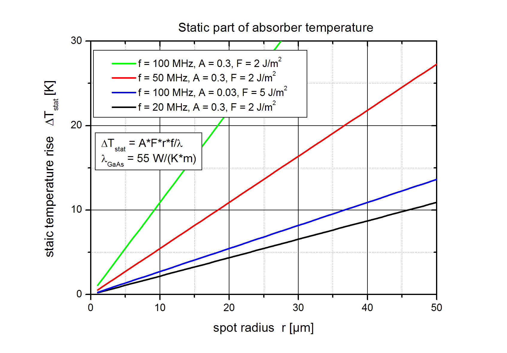
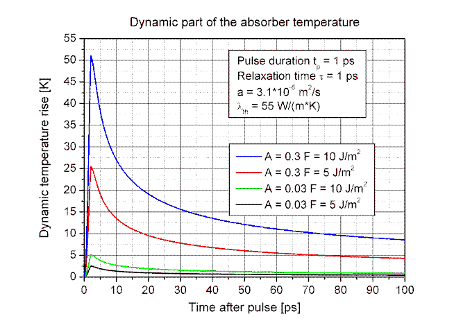
The maximum temperature rise decreases with increasing absorber relaxation time τ because the absorbed energy is released from the excited electrons into the crystal lattice after the relaxation time. If the relaxation time τ is longer then the pulse duration tp the electrons store the absorbed energy for a short time whereas the thermal energy diffuses already from the absorber layer into the substrate.
• Dispersion
Dispersion
The SAM consists of a Bragg mirror and an absorber layer with a certain optical thickness n·d in front of it. The interface between the semiconductor absorber and air builds a second Fresnel reflector. The absorption and the dispersion of the SAM depend on the following parameters:
- Surface reflectance Rs
- Optical absorber thickness n·d
- Absorption coefficient α.
Anti-resonant SAM
If the SAM is anti reflection (AR) coated ( Rs = 0 ) then the optical beam is solely reflected on the Bragg mirror. This results in a small dispersion similar as of a dielectric mirror.
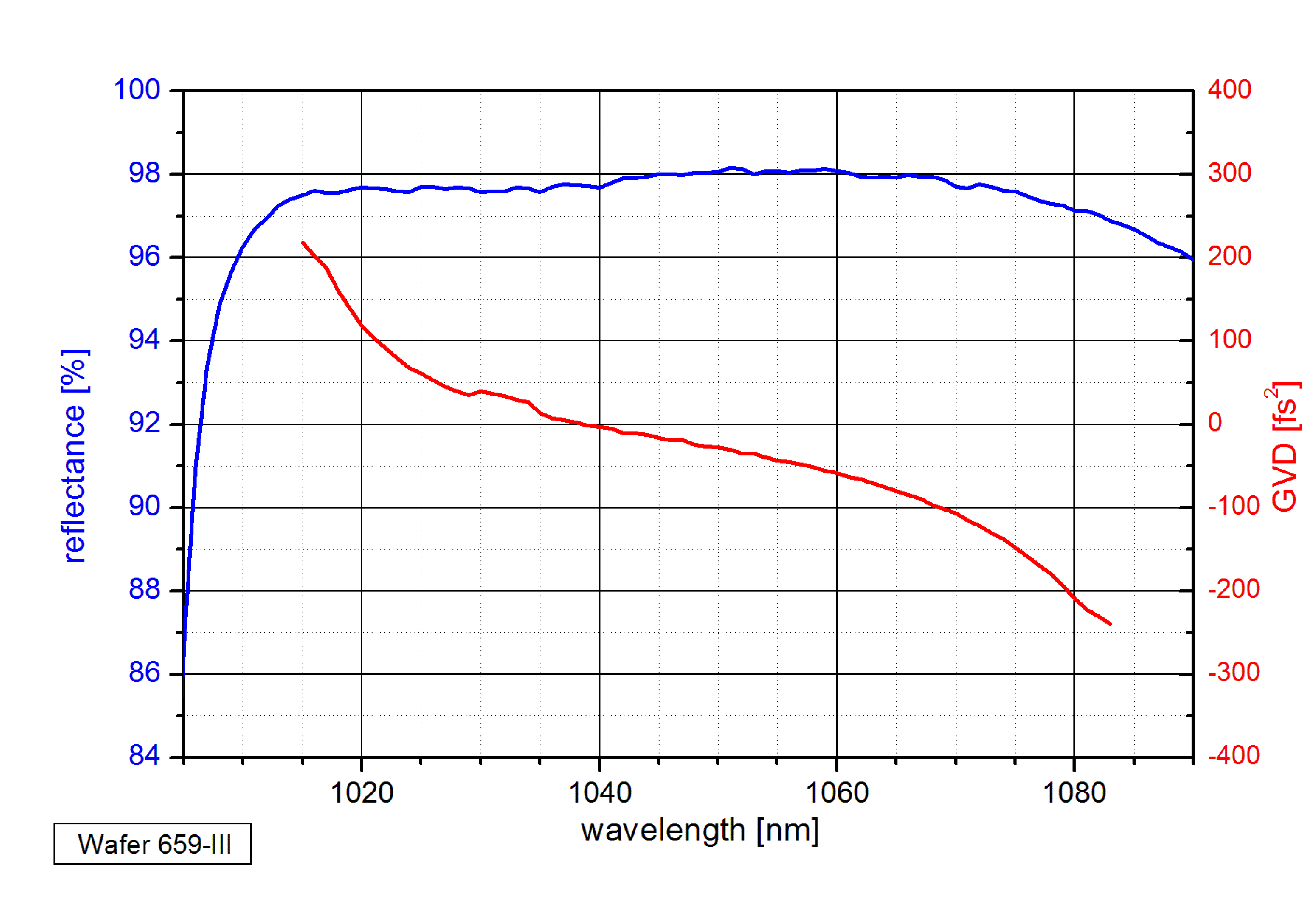
Group velocity dispersion (GVD) of an anti resonant SAM-1040-2-1ps.
The GVD is calculated using the second order derivative of the reflected phase.
For an anti resonant SAM the GVD is small in the spectral region of the stop band.
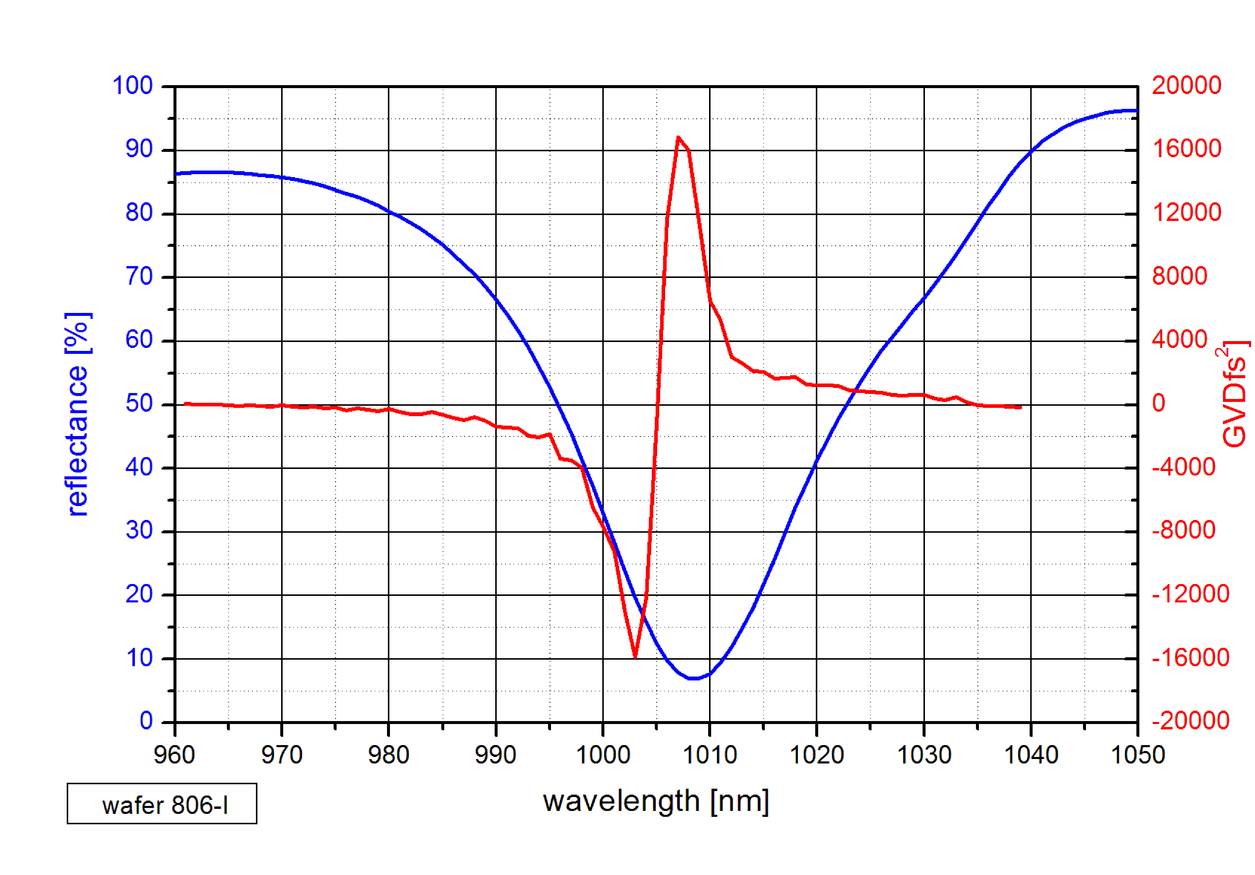
Resonant SAM
If the absorber layer is enclosed in a cavity determined by the Bragg mirror and the surface mirror with Rs > 0 then the light is partial reflected on both mirrors. The following two effects determine the net reflectance and the dispersion:
- The optical thickness n·d of the absorber layer.
- The absorption coefficient α of the absorber material.
Group velocity dispersion (GVD) of a resonant SAM-1030-32-3ps.
The GVD is calculated using the second order derivative of the reflected phase.
The largest absorption and the lowest reflectance is at the resonant wavelength λ = 2·n·d.
Around this resonance the GVD changes rapidly whereas outside the resonance the GVD varies slowly.
The amplitude of the GVD variation near the resonance increases with increasing optical thickness
n·d and decreasing absorption coefficient α of the absorber layer.